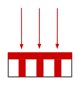
Electroplating
-
Up to 12 inches/300mm wafers
-
Large panel size electroplating possible
-
DPC: Direct Plating Copper
-
Cu, Ni, Au, AuSn, etc. electroplating.
-
Electroless plating for non-conductors using sputtered seed layers
-
Cu TSV (Through Silicon Via) fill
-
Cu TGV (Through glass Via) fill
-
Conformal TSV (Through Silicon Via)/ TGV(Through Glass Via) plating
-
Metal and solder electroplating

Electroforming
-
Fabrication of 3D metal solid structures using polymer or resist structures formed by X-ray lithography.
-
X-ray lithography with electroforming and molding know as the LIGA process.
-
High aspect ratio structures
-
Diameter as small as 1um, as thin s 20um
-
Huge applications in life sciences with biocompatible materials
-
Materials: Ni, Pd-Ni, Ni-Co
Applications
-
Fabrication of Nickel molds/ masters for nanoimprinting/ injection molding
-
Microfilters
-
Micro meshes/ filters
-
Nebulizer for mist generation
-
Microlens array
-
Metal masks
-
Gratings
-
Micropore membranes
-
Microneedles
-
Microfluidic chips